
 日本語
日本語 中文
中文 Deutsch
 Español
R&D Center
Over 1,000 verification experiments from all over the world every year
The world’s only soldering research institutes (soldering labs) gather together the latest soldering machineries and a variety of soldering equipments. The lab develops the foundation and new methods of soldering technology with utilizing advanced analytical tools.
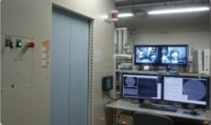
Micro X-ray CT
e.g. internal tip erosion and non-destructive inspection
Nano-focus X-ray CT
e.g. Non-destructive inspection of micro-voids in the soldering point
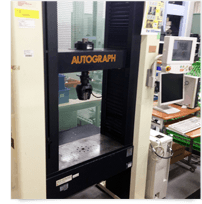
Tensile Strength Testing Machine
Bonding strength analysis
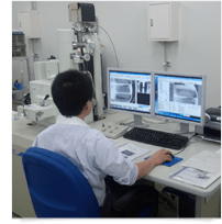
Analyzing soldering condition (SEM)
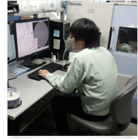
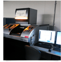
Observing PCBs and soldering tip(CT scan)
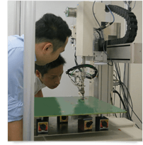
Experiments of robotic soldering
The number of soldering tests brought to us every day that we implement and verify totals over 1,000 per year. It includes unprecedented and exceedingly difficult orders that clients have been unable to find solution. Here are some analytical examples that soldering labs clarify and define the quality in soldering
Strength analysis of solder joints
Connectivity of substrate and soldered points
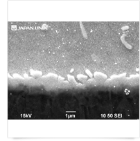
Analysis of intermetallic compounds
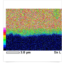
Observation of diffusion layer
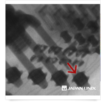
Non-destructive analysis of tips wettability
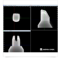
Inside of the new tip
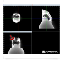
Erosion was found inside of the soldering tip (like cavity)
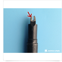
Abnormality unseen to the eye (analyzed tip)
Soldering condition of a sealed product
Checking for solderability in through holes
Through hole X-ray analysis
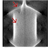
Found blow holes and voids that can not been seen from the outside
Our soldering lab employs specialized, experienced engineers with the latest tools and established soldering theories in order to meet the needs and challenges of a wide variety of customers.
Please contact us if you could consider our experience and skills in solving your problems.
Other Analysis Examples
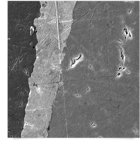
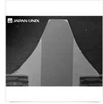
Aluminum plate soldering SEM analysis (x 1,000)

X-ray tracing image of soldering tips
Checking for inside erosions of soldering tips (like cavity)